The design of the remote controller is summarized here. This article shows how to design the omni-wheel robot’s schematic, including the circuit design of the IMU sensor and motor drivers.
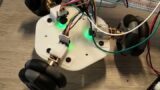
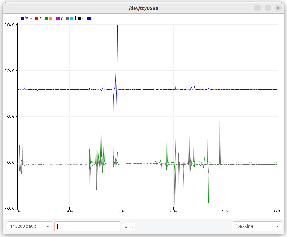
Test with breadboard
The tests with a breadboard were successful as in the video.
- Motors can rotate at a designated speed [rpm].
- IMU sensor could read translational acceleration and angular velocity.
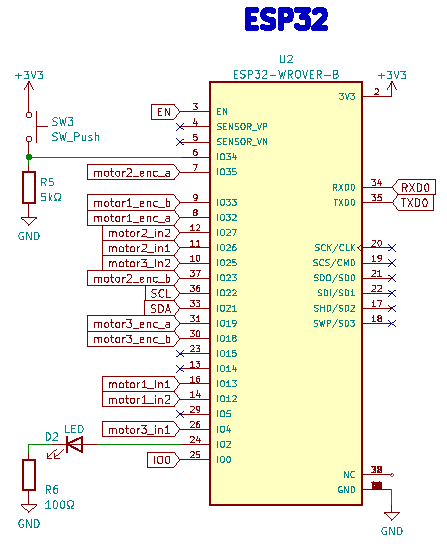
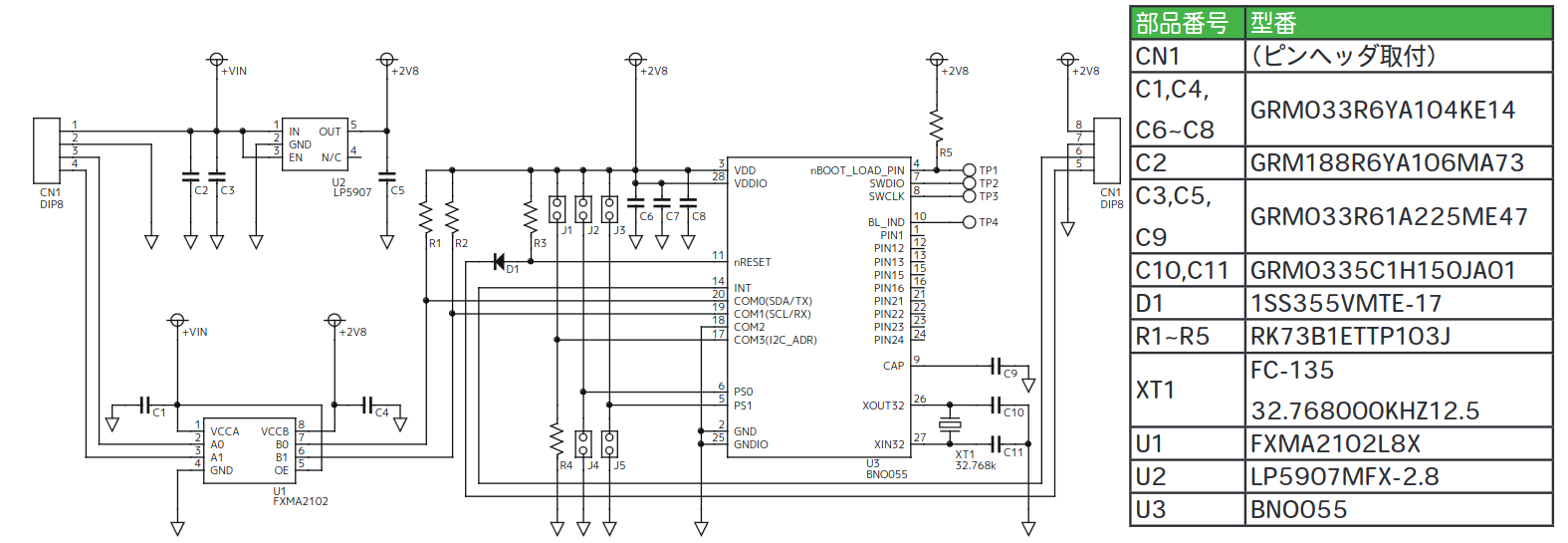
Overall schematic
The overall schematic is shown below.
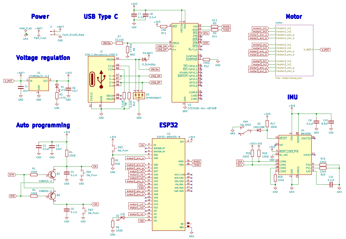
The meaning of each component is described in the following sections.
ESP32 PIN allocation
This site explains the PIN layout of ESP32 in detail.

From the citation, I determined each PIN role as follows.
| PIN | In/Out | Role |
| IO32 | Input | Motor 1 encoder hall signal A |
| IO33 | Input | Motor 1 encoder hall signal B |
| IO13 | Output | Motor 1 command input 1 |
| IO12 | Output | Motor 1 command input 2 |
| IO35 | Input | Motor 2 encoder hall signal A |
| IO23 | Input | Motor 2 encoder hall signal B |
| IO26 | Output | Motor 2 command input 1 |
| IO27 | Output | Motor 2 command input 2 |
| IO19 | Input | Motor 3 encoder hall signal A |
| IO18 | Input | Motor 3 encoder hall signal B |
| IO4 | Output | Motor 3 command input 1 |
| IO25 | Output | Motor 3 command input 2 |
| IO2 | Output | Debugging purpose LED |
| IO34 | Input | Debugging purpose tactile switch |
| IO21 | I/O | SDA signal for I2C communication |
| IO22 | I/O | SCL signal for I2C communication |
Motor
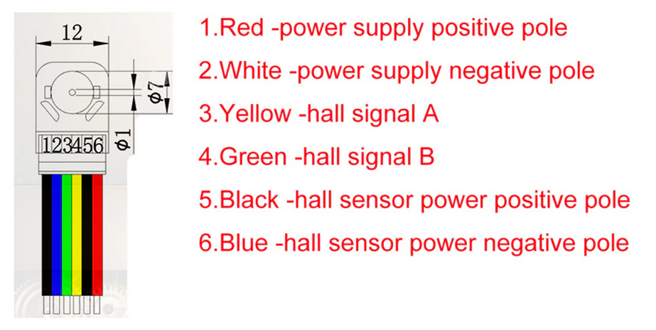
Each motor has to be connected to 2 encoder hall signal lines, 2 command input lines (by using 2 lines, we can control clockwise or counter-clockwise), and 2 power lines for the encoder.
Unusable PIN
As described in the site, IO15
must be HIGH during boot, prevents startup log if pulled LOW
ESP32 Pinout Reference
This means we cannot use IO15 as a motor command input because the PIN outputs HIGH in booting. Furthermore, IO14 had the same effect (when I use this PIN as a motor command input, the motor rotates unintentionally in booting). Thus, I avoid using those PINs.
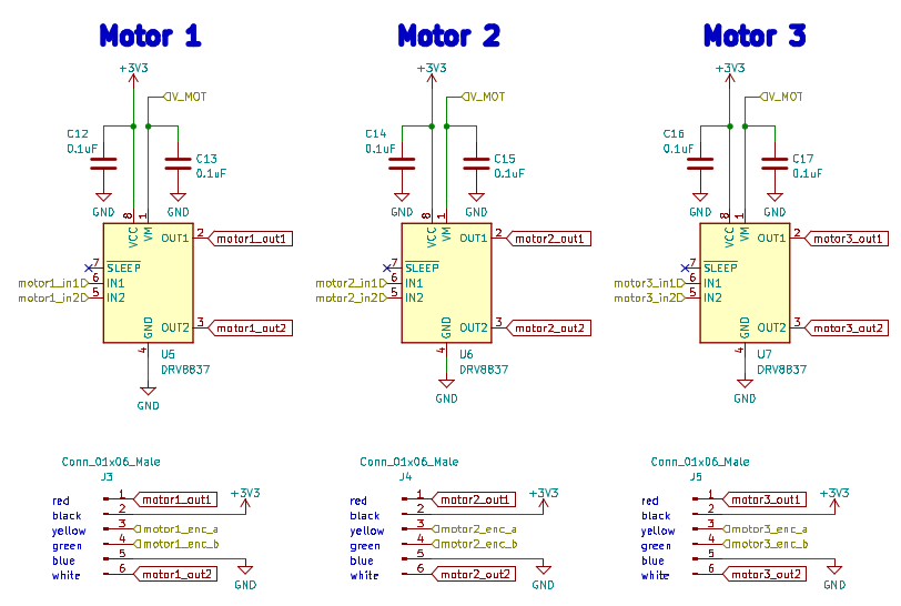
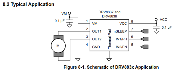
Motor driver
I am going to use DRV8837 (datasheet here) for this project.
In the breadboard testing, DRV8835 worked well and the maximum current capacity for DRV8835 is 1.5A, and that of DRV8837 is 1.8A. This shows that DRV8837 current capacity is sufficient. The manual for DRV8835 is here (in Japanese), and the following article summarizes how to use it.
Typical usage of DRV8837 is described below.
The relationship between motor wire color and the roles are summarized as follows (the original link here). The pitch length of the connector was 1.5mm, which is called as JST ZH connector.
The circuit schematic can be drawn like this based on the information above.
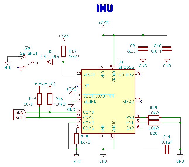
IMU
Previously, I used BMX055 as an IMU sensor when designing a circuit board for a drone, however, the product is not manufactured anymore. Thus, BNO055 was chosen at this time (the subsequent model of BMX055).
The following three sample circuits were found on the internet.
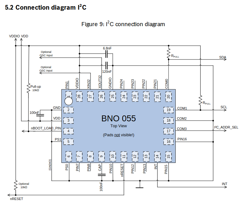
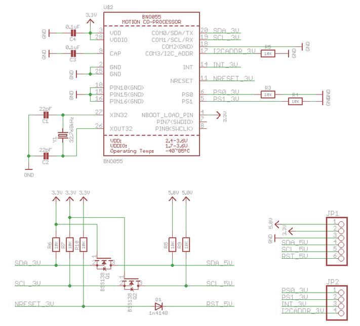
Design guidelines
The following conditions should be met (Table 5-1: Pin description in the datasheet explains the ideal PIN connection).
- An internal crystal oscillator is necessary only when the application requires great accuracy. Our application does not require an oscillator.
- PS0 and PS1 should be grounded to utilize the I2C communication protocol.
- COM3 is a PIN for the I2C address selection. We connect it to the ground with the 10kΩ resistor aligning with the example circuits.
- COM0 and COM1
- COM0 and COM1 stand for SDA and SCL, respectively.
- The PINs do not require a level shifter since the logic level of BNO055 is 3V0 and that of ESP32 is 3V3; those are close enough for I2C communication compatibility (perplexity link).
- Both lines should be connected to VDDIO externally via pull-up resistors so that they are pulled HIGH when the bus is free.
- The SDA and SCL lines should meet the following for noise reduction. Otherwise, the I2C transmission becomes unstable. This was found out by the breadboard analysis.
- The lines should not be close to each other or long.
- The PCB should have the ground plane.
- BL_IND corresponds to PIN10, which should connect to the GND.
- nBOOT_LOAD_PIN should be connected to 3V3 to boot in application mode.
- INT pin relates to interruption. Not required to be connected.
- nRESET PIN is usually set as HIGH, however, the pin should be LOW when booting in CONFIG mode. CONFIG mode is used to configure BNO, wherein all output data is reset to zero and sensor fusion is halted (this behavior holds in the breadboard analysis).
The circuit diagram for the IMU is as follows.
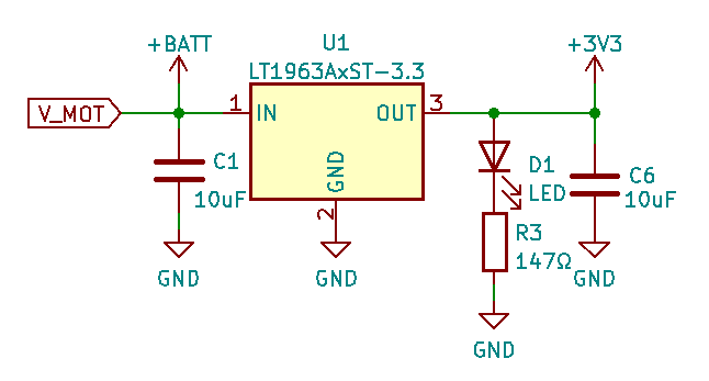
Other components
Other components are nearly the same as the remote controller circuit. The only difference is that a battery needs to be connected directly to motor drivers through V_MOT.
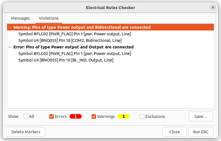
Electrical rules check
The circuit has 4 rule violations according to the checker but I ignore these warnings since it aligns with the above three circuit examples.
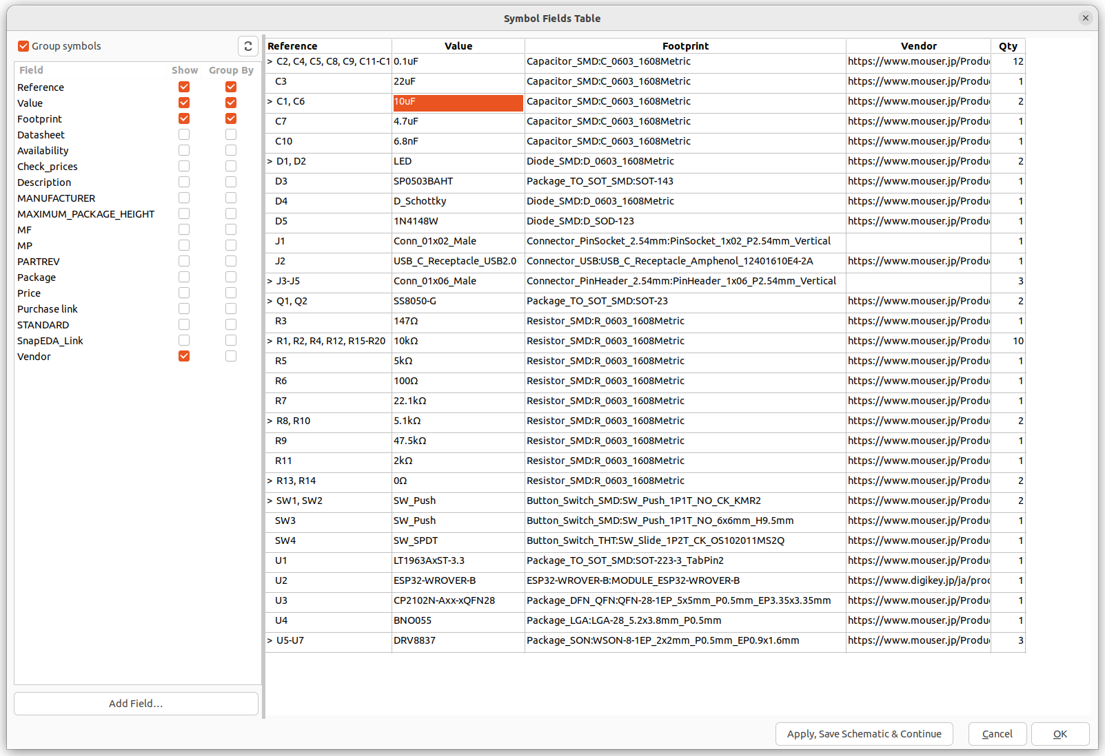
Footprint assignment and output BOM file
After completing the following procedure,
- Open “Tools -> Annotate Schematic…” and click Anotate button.
- Open “Tools -> Assign Footprints…” and assign footprints.
- Open “Tools -> Edit Symbol Fields…” and fulfill the Vendor.
we can get the following table.
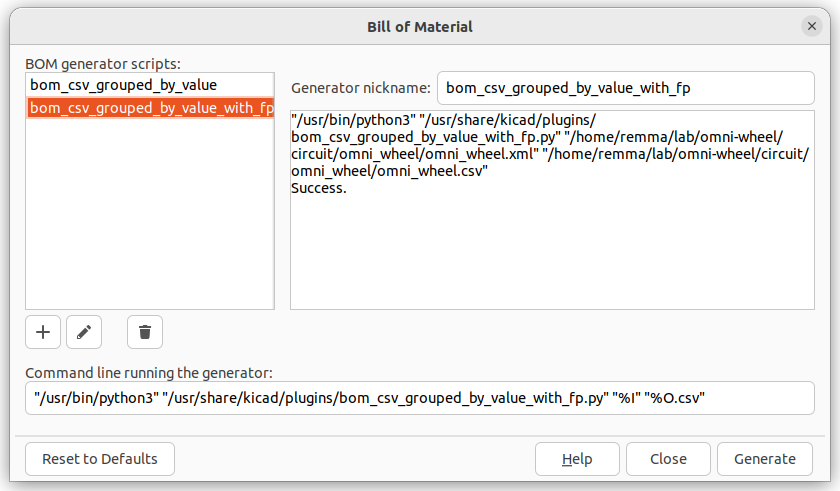
Finally, we get the BOM file by “Tools -> Generate BOM…” (Caution: you need to remove the previously created .csv file before you execute this process).
Summary
I have finalized the schematic in this article. Reading the circuit design guidelines of the IMU sensor from the datasheet was hard work for me… The PCB design is going to be addressed in the following article.
コメント